
Advanced Packaging

2026 Forecast of China’s Advanced Packaging Capacity as a Global Share
China’s role in advanced packaging is moving from “important participant” to “strategic balancing force” in the global semiconductor supply chain. By 2026, its capacity is expected to represent a meaningful share of worldwide advanced packaging output, especially in high-volume OSAT-driven segments, even as some of the most cutting-edge AI packaging still remains concentrated elsewhere. That contrast is exactly what makes the story interesting: China is scaling fast, but the global market is not all one market. Different packaging technologies, different end markets, and different levels of localization are expanding at very different speeds.

D2D Interface Bandwidth and Latency Comparison in Chiplet Architectures
Chiplet architecture has turned the package into a real performance battleground. Once multiple dies are placed side by side or stacked within the same advanced package, the quality of the die-to-die, or D2D, interface becomes one of the most important determinants of system behavior. Bandwidth is no longer a nice-to-have metric, and latency is no longer a small implementation detail. Together, they shape whether a chiplet system feels nearly monolithic or frustratingly fragmented.
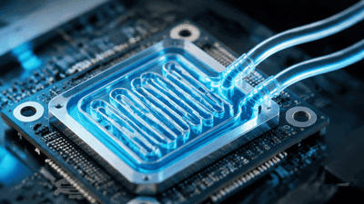
Thermal Management in Heterogeneous Integration: Embedded Microfluidic Cooling Solutions
Anyone who has opened a laptop after a long gaming session knows that heat is the silent enemy of electronics. Now imagine that same problem in a package holding multiple high-power chiplets, stacked dies, and dense memory, all squeezed into a few square centimeters. That is the world of heterogeneous integration—and it is brutally hot. Traditional cooling methods are being pushed to their limits, and that is where embedded microfluidic cooling starts to sound less like a futuristic research topic and more like a practical necessity.
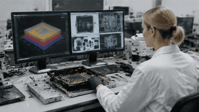
Value Distribution of Advanced Packaging via AI Chip Teardown Analysis
If you want to understand where the real value sits in modern AI hardware, teardown analysis is one of the best tools available. Once you open up a flagship AI accelerator and examine its layers, you quickly discover that the package is no longer a supporting actor. It is a major source of cost, performance, and strategic value. In many cases, advanced packaging now accounts for a surprising share of total device value, rivaling or even surpassing the logic die in importance once HBM, interposers, substrates, and assembly are included.
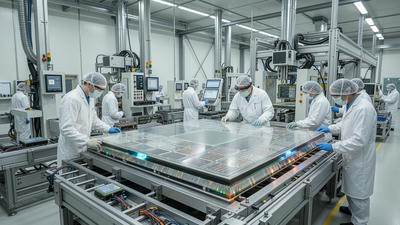
The Critical Role of Silicon Interposers in Large-Size AI Chips
When people talk about the future of AI chips, the conversation usually starts with transistor nodes, model sizes, or memory bandwidth. But behind all of that sits a less glamorous, yet absolutely decisive, piece of technology: the silicon interposer. In large-size AI chips, the interposer is what makes heterogeneous integration practical at scale, tying together massive compute dies, multiple HBM stacks, and increasingly complex chiplet ecosystems into one high-performance package.
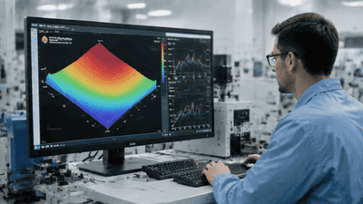
Warpage Control in Advanced Packaging: The CTE Matching Challenge
Advanced packaging has made semiconductor systems more powerful, denser, and more flexible than ever, but it has also exposed a stubborn mechanical problem that refuses to go away: warpage. As heterogeneous integration pushes more dies, more layers, and more materials into a single package, the question of how those materials expand and contract becomes central to yield, reliability, and manufacturability. At the heart of that problem is coefficient of thermal expansion, or CTE, matching.
Techno-Economic Comparison of 2.5D vs. 3D Packaging: Which to Choose When?
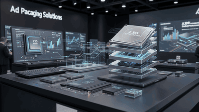
Advanced packaging has become the place where semiconductor scaling is now negotiated, and two of its most important options are 2.5D and 3D packaging. Both are powerful forms of heterogeneous integration, but they solve different problems, carry different risks, and make sense at different points in a product roadmap. The real question is not which one is better in the abstract. It is which one gives the best balance of performance, cost, yield, thermal behavior, and manufacturability for a specific system.

New EDA Challenges and Tool Iterations Driven by Advanced Packaging
Advanced packaging has changed the semiconductor design flow in a way that feels subtle at first and then suddenly unavoidable. What used to be the back end of the line—package selection, assembly, and test—has become a co-equal design domain alongside logic, memory, and interconnect. As heterogeneous integration moves from a niche practice to the default architecture for high-end AI, HPC, networking, and mobile systems, EDA tools are being pushed far beyond their traditional boundaries.
TSV Cost Structure and Yield Ramp-Up in 3DIC
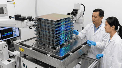
Through-silicon via, or TSV, technology sits at the heart of many advanced packaging and heterogeneous integration roadmaps. As the industry moves from 2D scaling to 3D integration, TSVs enable vertical stacking of dies, shorten interconnects, raise bandwidth, and improve system performance. Yet behind the impressive technical benefits lies a complex story of cost structure, yield ramp, and manufacturing learning curves that determine how quickly 3DIC can become mainstream in high-volume production.

2026 Global Advanced Packaging Market Exceeds $60B – Supply Chain Breakdown
The advanced packaging market has entered a new phase. In 2026, global revenue is expected to exceed $60 billion, a scale that would have seemed surprisingly high only a few years ago. What changed is not just demand, but the nature of demand itself: AI accelerators, high-bandwidth memory, chiplets, and heterogeneous integration have turned advanced packaging from a niche technology into a core growth engine for the semiconductor industry. The headline number is impressive, but the real story is the supply chain underneath it.